This is the Revision A verion of the Compass360 RoboBrick. The status of this project is that it has been replaced by the CompassDT1 RoboBrick.
This document is also available in PDF format.
The Compass360 RoboBrick uses a 1625 analog compass module from Dinsmore Instrument Company to detect magnetic bearing with a resolution approximately 8 bits. You should be informed that the magnetic enviroment inside dwellings can induce substantial errors in magnetic bearing of more than 10 degrees. (You have been warned!)
There is no programming specification yet.
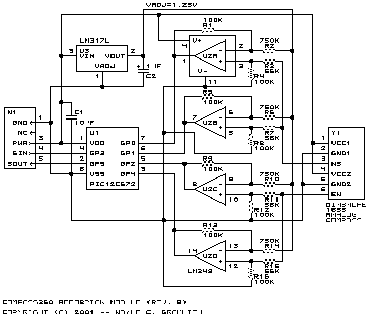
The hardware consists of a circuit schematic and a printed circuit board.
The schematic for the Compass360 RoboBrick is shown below:
The parts list kept in a separate file -- compass360.ptl.
The printed circuit board files are listed below:
There is no software yet.
Any fabrication issues that come up are listed here.
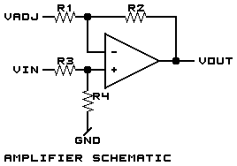
In order to understand how the resistors around the operational amplifiers are picked it is necessary to analyze one of the amplifier cicuits. We'll do the analysis the amplifier below:
Let's call Vin the input voltage to R3 and Vadj the adjustment voltage input to R1.
V+ is the voltage input to the positive side of the operational amplifier and V- is the input to the negative side. The trick with operational amplifiers is that they have very high input impedances; hence, the current into and out of both the V+ and V- terminals is assumed to be zero. In addition, since we have a properly designed feedback circuit, the operational amplifier will work like crazy to keep V+ and V- equal to one another; thus, we just assume that V+ is always equal to V-. These assumptions are summarized as:
(1) V+ = V-
(2) IV+ = 0
(3) IV- = 0
R3 and R4 form a simple voltage divider of Vin:
(4) V+ = VinR4/(R3 + R4)
The voltage drop across R1 is:
- (5) VR1 = Vadj - V-
- = Vadj - V+
- = Vadj - VinR4/(R3 + R4)
Using Ohm's law, we can compute the current through R1 as:
- (6) IR1 = VR1 / R1
- = [Vadj - VinR4/(R3 + R4)] / R1
- = Vadj/R1 - VinR4/[R1(R3+R4)]
Since there is no current into V-, the current through R2 is the same as the current through R1:
(7) IR2 = IR1
The voltage drop across R2 is computed using Ohm's law as:
- (8) VR2 = IR2R2
- = IR1R2 =
- = [Vadj/R1 - VinR4/[R1(R3+R4)] ]R2
- = VadjR2/R1 - VinR2R4/[R1(R3+R4)]
The voltage out (Vout) is:
The equation can be rewritten as:
- (9) Vout = V- - VR2
- = V+ - VR2
- = VinR4/(R3 + R4) - [VadjR2/R1 - VinR2R4/[R1(R3+R4)] ]
- = VinR4/(R3 + R4) - VadjR2/R1 + VinR2R4/[R1(R3+R4)] ]
- = VinR4/(R3 + R4) + VinR2R4/[R1(R3+R4)] - VadjR2/R1
- = Vin[R4/(R3 + R4) + R2R4/[R1(R3+R4)] ] - VadjR2/R1
- = Vin[R4/(R3 + R4) + (R2/R1)×R4/(R3+R4)] - VadjR2/R1
- = Vin[R4/(R3 + R4) × (1 + R2/R1)] - VadjR2/R1
- = Vin[(1 + R2/R1) × R4/(R3 + R4)] - VadjR2/R1
(10) Vout = Vin × G - Voffwhere the amplifier gain is G:
(11) G = (1 + R2/R1) × R4/(R3 + R4)and the voltage offset is Voff:
(12) Voff = VadjR2/R1
For the first iteration of resistor values, we want the amplifier to take the voltage output from the Dinsmore 1655 analog compass module of 1.9 to 3.1 volts and convert that to a voltage swing of 0 to 5 volts (Vcc).
Let Vlow lowest input voltage and Vhigh be the hight input voltage. What we want is:
- (13) Vout = (Vin - Vlow)[Vcc/(Vhigh-Vlow)]
- = Vin[Vcc/(Vhigh-Vlow)] - Vlow[Vcc/(Vhigh-Vlow)]
Matching to equation (13) to equation (10) in the previous section, the gain (G) is:
(14) G = Vcc/(Vhigh-Vlow)and the voltage offset (Voff) is:
(15) Voff = Vlow[Vcc/(Vhigh-Vlow)]
Starting with the voltage offset:
Now combining equations (16) and (12) from the previous section, we get:
- (16) Voff = Vlow[Vcc/(Vhigh-Vlow)]
- = 1.9 [ 5 / (3.1 - 1.9) ]
- = 1.9 ( 5 / 1.2 )
- = 1.9 × 4.17
- = 7.92
(17) Voff = VadjR2/R1
At this point we have to pick a value for Vadj. Initially, I tried to set Vadj to Vcc, but when I worked through the equations, R4 had a negative value. Since I can not buy negative resistor values, I decided to drop Vadj down a little. At Vadj equal to 2.5 volts, it started to work, but R3 had a very small value. The lower Vadj was dropped, the more reasonable the value of R3 was. I ultimately decided to set Vadj to 1.25 volts because an LM317L will produce that voltage without needing any trim resistors.
Now substituting in values for Voff and Vadj we get:
(18) 7.92 = 1.25 × R2/R1or
(19) R2/R1 = 7.92 / 1.25 = 5.83I'll pick R1 to be 100K Ohms thereby getting:
(20) R2/100K = 5.83or
(21) R2 = 583KWe'll round that down to 560K Ohms.
Now switching over to the gain side of the equation:
Now combining equation (22) with equation (11) from the previous section, we get:
- (22) G = Vcc/(Vhigh-Vlow)
- = 5 / (3.1 - 1.9)
- = 5 / 1.2
- = 4.17
(21) G = (1 + R2/R1) × R4/(R3 + R4)and substituting for G, R1 and R2 we get:
Picking R4 to be 100K, we can trivially solve for R3:
- (22) 4.17 = (1 + 560K/100K) × R4/(R3 + R4)
- = (1 + 5.6) × R4/(R3 + R4)
- = 6.6 × R4/(R3 + R4)
- (23) .63 = R4/(R3 + R4)
R3 is rounded down from 59K down to 56K.
- (24) .63 = 100K / (R3 + 100K)
- (25) .63 × (R3 + 100K) = 100K
- (26) R3 + 100K = 100K / .63 = 159K
- (27) R3 = 159K - 100K = 59K
Thus the final values are:
- R1 = 100K Ohms
- R2 = 750K Ohms
- R3 = 56K Ohms
- R4 = 100K Ohms
- Vadj = 1.25 Volt